Thursday, July 8, 2010

Hacking the Wii MotionPlus

So its been two days since I got my Nintendo Wii MotionPlus (henceforth simply ‘WM+’; yeah, I know I called it the ‘M+’ earlier :-|) clone from DealExtreme. And I’ve been itching to get some data off it.

The WM+ uses I2C to send and receive data from a host, which is normally a WiiMote, but in my case it is a PIC16F877.
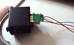
The hacked WM+. I desoldered the pass-through port (normally used to connect a Wii Nunchuck) and used it as a mating female connecter for the WM+’s male connector.

On the net, I couldn’t find a single site that used a PIC as the host. And most sites had code specific to the microcontroller used by the site’s creator (which was more often than not an Arduino). So after cracking my nut trying to figure out what in the heck these Arduino chaps were doing, I decided to post pseudo-code so that others working with the WM+ can easily write code for their micros.

*        *        *

Pseudo-code:

//initialize the WM+
i2c_start
i2c_write(0xA6)
i2c_write(0xFE)
i2c_write(0x04)
i2c_stop
  
//read data
while(true)
{
    i2c_start
    i2c_write(0xA4)
    i2c_write(0x00)
    i2c_stop
   
    i2c_start
    i2c_write(0xA5)
    yaw_lo_byte = i2c_read(ack)
    roll_lo_byte = i2c_read(ack)
    pitch_lo_byte = i2c_read(ack)
    yaw_hi_byte = i2c_read(ack)
    roll_hi_byte = i2c_read(ack)
    pitch_hi_byte = i2c_read(nack)
    i2c_stop
   
   
//this is necessary since the last two bits
    //in the high bytes are useless

    roll_hi_byte = roll_hi_byte >> 2
    pitch_hi_byte = pitch_hi_byte >> 2
    yaw_hi_byte = yaw_hi_byte >> 2
   
    //send to computer for displaying
    putc
    printf
}

A few words about the pseudo-code. You’ll find that the hex value that you write in line 3 is 0xA6. Some websites say the WM+ ‘starts off at address 0x53’. This is confusing since 0xA6 is not equal to 0x53. To figure this out you need to know a little about the I2C protocol.

*        *        *

A little about I2C:

Quite often, I2C devices use 7-bit addressing, and a 1-bit read/write indicator. 7+1=8 bits=1 byte. All I2C communications start with the host sending a ‘start condition’, followed by the 7-bit address, followed by a 1 or a 0, telling the device that data is either to be written to, or read from that address. This may be followed by additional reads or writes. Between reads and writes, an ‘acknowledge (1)’ or ‘not acknowledge (0)’ is sent. Communication is terminated with a ‘stop condition’.

*        *        *

Anyway, so how is 0x53 equal to 0xA6? Simple. 0x53 is the address that we want to write to. So the first seven bits are 0x53, and since we are writing the next byte, we send a 1. In C this is written as:

(0x53<<1)+0

Which, in plain English reads as: “Shift 0x53 to the left by one bit; set the least significant bit to 0”.

Now we see that (0x53<<1)+0 = 0xA6. Do it yourself if you’re not convinced!

So once the WM+ is initialized, one can start reading gyro data. Some sites recommend that you wait 38ms before reading data, since the WM+ needs to initialize fully, but I haven’t done that and yet my WM+ gives me ‘nice’ data.
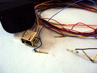
DSC00644 Close-up of the pass-through port female connector. Only four wires are needed. Red – Vcc; Black – Ground; Blue – SCL; Yellow – SDA. The pins that go into the bread board are scavenged from a broken DB25 male plug.

Gyro data is stored in six consecutive address. In my while loop, I set the address from which to start reading data from – this is 0x52 (which becomes 0xA4, since we’re writing). I write 0x00 to the register to indicate I ‘want’ data. Then I read data into the ‘hi’ and ‘lo’ bytes of the roll, pitch and yaw variables. Data reads are ‘ack-ed’, ie, acknowledged. The last byte is ‘nack-ed’. This is NOT to say that it is not acknowledged, rather the word ‘not’ in ‘not acknowledge’ actually refers to Boolean inversion. Since an ack is binary 1, a nack becomes binary 0.

In my actual code, I have a for loop inside the while loop. The for loop runs 32 times to average out the roll, pitch and yaw readings. After averaging, the data is sent out using a string of putc statements. Alternatively, printf may be used to print to a terminal program – the choice is yours. Infact, I threw together a simple LabVIEW program to display the roll, pitch and yaw on a dial. You can see that I am simultaneously also graphing the results.

Roll Pitch Yaw
The LabVIEW frontend. Roll, Pitch and Yaw are depicted.

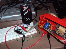
My setup is pretty simple – just a PIC16F877 with the TinyBootloader on it, running at 20MHz; a MAX232 for serial comms; the PICKit2 provides 5v power to the PIC and the MAXIM chip; a TI LP2950 regulates the 5v to a safe 3.3v for the WM+. A cheap USB-to-Serial dongle is used to receive data @ 115.2Kbaud.

  The current setup - WM+ connected to a PIC16F877. Power provided by the PICKit2. Serial data sent to LabVIEW through a MAX232 and USB-Serial dongle.

I still need to calibrate the WiiMote, and see how accurate the data is. In the next few days I’ll be making my data acquisition board wireless (by including the RF code from an earlier project, and using a Li-ion battery). I’ll be going around the place, sticking the board to swivel chairs, on the wheel of a cycle, on a treadmill, to a fan blade, and whatever else I can think of :-P.

Updates, more pics and videos will be up in a while.


Credits:

Monday, July 5, 2010

I Love the Mailman

I think certain clarifications are in order - I am completely heterosexual; its just that today, one of the mailmen brought me a few parcels, which I have been eagerly waiting for. One of those parcels was a Sensiron SDP610 sample, which is a CMOS differential pressure sensor; the other parcel is the subject of this blog.

1 2
Left: The Sensirion SDP610 differential pressure sensor
Right: A Nintendo Wii MotionPlus clone

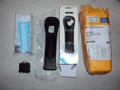
I’m building a quadrotor, and after doing a bit of searching online, found that IMUs cost a bomb. Not wanting to spend $$$ on commercial units I decided to go the DIY way. I got onto DealExtreme and purchased a Wii MotionPlus clone (hereafter simply ‘M+’). The original M+ was made by Nintendo (of the Super Mario/Contra/Space Invaders fame), as an accessory for its Wii gaming console.

The Wii revolutionized the way the world played video games. Nintendo introduced a motion controlled gaming device that took the world by storm. However soon, gamers wanted more, and when they found that the WiiMote controller gave inaccurate results when moved vigourously, they decide to add a piggy-back module to the controller.

The M+ is a 3 axis gyroscope to complement the 3 axis accelerometer already in the WiiMote. Simple maths says 3+3=6; the M+ coupled with the WiiMote gives a complete 6DOF motion controller, using which you can 'swing’ a simulated golf club, or ‘throw’ punches at the world’s deadliest boxer, maybe even ‘play’ a game of pool.

So I spent USD12~INR550, and DX shipped me the M+ along with a complimentary rubber sleeve to protect my (inexistent) WiiMote. Shipping was free, and was done via registered mail. The package took 23 days to ship from HK to Gurgaon, India.

Packaging was good – the M+ came plastic wrapped in a product box. The outer packaging was a bubble mailer. No damage other than a few wrinkles on the box’s surface.

3Good packaging by DX 

Also included in the product box were ‘documentation’ and leaflets – they’ll go straight to the raddi pile to be sold as scrap paper since I can’t read Chinese. Thoughtful of the manufacturers, but useless to me :-|

5
Decent build quality

The M+ itself looks solid, and build quality is good – no loose bits or clamps (not that it really matters since I’m gonna tear it apart anyway). The M+ presented me with a small problem – it was held together by tri-wing screws. Not one to be outsmarted by two screws, I took a small flathead screwdriver and gently got the screws out.

6 
The tri-wing and the flathead that got it out.


The pieces

Here are the innards of the M+:

 
The upper side of the PCB. Visible on the top left corner is the IXZ650 gyro. The black epoxy in the centre covers the microcontroller, in a CoB construction style. The connector is to the left, while the expansion port is to the flat cable on the right.

The bottom side of the PCB. In the centre is the IDG650. On the top right is what seems like an EEPROM chip.

It seems funny why the clone would have two 2-axis gyros when just a 2-axis and a 1-axis would suffice. I guess I’ll have to get my hands dirty to see if there’s any difference in its functioning.

Updates in a bit.

Thursday, July 1, 2010

No Strings (or Wires), Attached

It’s been a while since I’ve blogged. Its not like I haven’t been trying – my drafts pane in Windows Live Writer is full of half-finished posts. Maybe I’ll complete them and post them before the summer ends. Or maybe not.

This post is about using those cheap 300-bucks-a-pair modules. For international readers, INR300~USD6. If you look around where you live you’ll find the same or similar modules which do the same thing. Sparkfun carries these variants:
http://www.sparkfun.com/commerce/product_info.php?products_id=8946
http://www.sparkfun.com/commerce/product_info.php?products_id=8947

SeeedStudio stocks these:
http://www.seeedstudio.com/depot/433mhz-rf-link-kit-p-127.html?cPath=101_103

The difference between Sparkfun’s and Seeed’s is that the former has a receiver that is PLL synthesized, and the latter uses a relatively cheaper, albeit less reliable LC circuit. I have both types of modules, bought locally. Both types use a SAW resonator for transmission.

These dirt cheap RF modules work at 433MHz (you’ll also find the 315MHz variety), which puts them squarely in the ISM transmission band. They use ASK modulation to send data across. You can mix and match PLL/LC transmitters and receivers without a problem, just so long as they’re all on the same frequency (duh!).

A lot of people use these modules for low cost wireless control mainly because they’re a breeze to interface. The easiest way to work with the modules is to buy the HT12-E and HT12-D encoder-decoder pair. These chips are essentially parallel-to-serial shifters and output a user set 8-bit ‘address’ along with 4-bits of useful data.

But what if you want to send more that just 4 bits? Suppose you want to send an arbitrary text string? Or maybe the 8-bit brightness value of a wireless night lamp? In such situations these chips are useless. You could buy the HT640-HT648 encoder-decoder pair, but again, that would limit you to 8-bits of data at a time.

The best option (IMHO) is to use microcontrollers as the encoder and decoder. Using a micro will, in a manner of speaking, allow you to kill several birds with one stone. You can use the same micro to decode the received data, as well as perform control functions at the RX end.

So how do you go about using a micro? I’ll start at the beginning:

The reason why these modules are cheap is because they are very simple. They are, at most, just a crude pipe through which RF data passes. There is absolutely no form of error correction, no data protocol whatsoever, and certainly no guarantee of data transmission.

One of the biggest problems these modules suffer from is that of DC-drift. Think of digital data being passed through a series capacitor. Let us say that you try to send several 1s, the capacitor will soon charge up until it is saturated. Once it gets saturated you can’t transmit data any longer, since there is no charge mobility. Similarly if you send a long string of 0s the capacitor will get discharged, and again, you won’t be able to transmit data. The trick is to send a balanced number of 1s and 0s. Over a short period of time, if the number of 1s is equal to the number of 0s transmitted, then the ‘DC level’ of the RF module remains balanced.

Clever, you say. But how do I put this into practice? You could use the Manchester encoding scheme to transmit data. Put very simply, in Manchester encoding, each bit is encoded as two bits. A 1 is encoded as binary 01, and a 0 is encoded as a binary 10. Thus, regardless of what data is sent, the transmission is DC-balanced.

A very obvious disadvantage is that the data rate is immediately halved (or one can say that the bandwidth doubles). There are more complex coding schemes which are more bandwidth efficient such as 8B/10B encoding, but I’ve stuck with Manchester encoding, since it’s much easier to do.

Now I didn’t really do any Manchester coding or decoding – I used a bit of a cheat. Most micros have a UART as well, so I included that too in my ‘hack’ – using built-in hardware to do dirty work greatly reduces my effort :-) Since I’m using the UART, I can only send 8-bit chunks of data. The data transmitted must satisfy these conditions:

  • Data is to be balanced, so each byte should have four 1s and four 0s.
  • There should be no more than two consecutive 1s or 0s. This is a constraint which ensures that data is Manchester-like.

Of the 256 possible numbers, there are 26 8-bit binary strings that fulfil the above criteria. I’ve arranged the numbers in Gray-code-like order.

00110011   0x33
00110110   0x36
00110101   0x35
00101011   0x2B
00101101   0x2D
01100110   0x66
01100101   0x65
01101010   0x6A
01101001   0x69

01010011   0x53
01010110   0x56
01010101   0x55
01011010   0x5A
01011001   0x59
01001011   0x4B
01001101   0x4D
10100110   0xA6
10100101   0xA5

10101010   0xAA
10101001   0xA9
10110010   0xB2
10010011   0x93
10010110   0x96
10010101   0x95
10011010   0x9A
10011001   0x99

 
Each yellow number corresponds to a particular hexadecimal number from 0x0 to 0xF. Thus there are 16 ‘yellow numbers’. Each byte that I want to transmit can be broken into two nibbles. Each nibble is encoded using one of the numbers highlighted in yellow. So, for each nibble, I transmit a DC-balanced byte. At the receiving end the nibbles are collected and ‘re-formed’ into bytes. Clearly, the transmission rate is half of the data rate.

When using this scheme a few other things need to be kept in mind. The transmitter will only be turned on when transmitting data. However, the receiver is always on. And that’s a problem. The receiver will happily ‘lock-on’ to the strongest RF signal it can find. It doesn’t care if that signal is meaningless data – it will demodulate whatever it finds. So as it sits there, the receiver is demodulating junk. Suppose we now start sending data, how does the receiver UART know that this infact, is actual data, and not junk?

The way to solve this is to first send a ‘look-at-me’ sequence. The LAM sequence is just a series of balanced numbers sent by the transmitter to ‘wake’ it up. By doing this, the transmitter establishes itself as the strongest signal source. The LAM also serves as a kind or reference for the receiver’s UART to ‘lock’-onto. After much trial and error, and forum searching, I found that the LAM sequence of 0xBA 0xBE 0xFA 0xCE (or hex BABE FACE) works wonderfully, though it is NOT balanced!

After the LAM, a ‘start’ code is sent (I use the numbers in green, but any sequence may be used). Only once the ‘start’ is received does the receiver accept further data.

The data is followed by a simple checksum. The checksum is the 8-bit sum of all the data. If the checksum calculated at the receiver is not the same as the checksum transmitted, then it implies that some data has been lost in transmission.

Transmission ends when the number 0x99 (red) is received.

I am still working on error checking using data prediction. I’m also working on making this code adaptable to use in a multi-transmitter setup using arbitration.

The code in its current form is very robust and works very well. My setup has two transmitters and one receiver. One transmitter causes a red LED to blink on the receiver side; the other make a white one blink. Understandably, there are times when the transmitters interfere, but this doesn’t cause spurious results.

As testament to the robustness of the protocol (and maybe even the transmitter modules!) here is some data: though the datasheet specifies using a λ/4 monopole antenna (approx 17cm of wire @433MHz or 23cm of wire @315MHz), both transmitters and receivers are happily TX-ing and RX-ing without any external antennae. I suppose I could increase range and reliability by sticking on a wire, but I’m getting a 10m range with a 1.5v battery!

If you want the code ask in the comments. I’ll be posting pics of my setup soon.

Tuesday, February 16, 2010

Touch Me Please: Video

You can watch the video of my touchpad interface here:

The touchpad is taken from an HP Pavilion dv2000 laptop. A PIC16F628A performs all the necessary PS/2 host functions; and a Nokia 3310 LCD is used to display ‘mouse’ movement.

The LCD uses custom graphics. I wrote both, the LCD driver, and the firmware to run the touchpad. Code is in CCS-C. Both drivers are based on info found online. Do note, that the touchpad code on this page is slightly different from the touchpad code posted in the original page.

You can find the original post here.

Sunday, February 14, 2010

Touch Me Please!

Before I dive into this post I take a moment to profusely apologize for the title of the post – it is tragically horrendous.

OK, so now that I’ve got that out of the way, lemme begin. This post is a little out of ‘order’; it would have been more appropriate had I first blogged about how I procured some of the components mentioned in this post. But heck! Lazy as I am, I guess I’ll leave that for a later date.

A friend of mine (un)fortunately busted his laptop several months back. I managed to persuade him to let me scavenge parts from the laptop. What parts did I get? That’ll be the subject of a different post :-D I managed to rescue several components; a touchpad being one of them. And as usual, I went about trying to interface it.

Electronics being my love, and today being Valentine’s Day, it is most fitting that I have successfully managed to communicate with the touchpad. Now before you start making judgements about me, and why I fool about with electronics on this most awesome day, let me tell you how I went about the interfacing.

The touchpad is a mouse replacement ubiquitous on laptops. Synaptics is by far, the biggest touchpad manufacturer. Alps Electric, Cypress, and a few others are also into the touchpad market. Most touchpads today work on the principle of capacitive sensing.

The touchpad of my trusty IBM Thinkpad R51 

The touchpad I scavenged was from an HP Pavilion dv2000 series laptop. The touchpad used is probably manufactured by Alps Electric Corporation (there is a prominent “ALPS” silkscreened onto the back of the PCB). The touchpad is a capacitive sensing type and is controlled by a 48 pin QFP. The chip is marked 1CA026A. I googled high and I googled low but I couldn’t find anything useful; no datasheets, nothing. So it became necessary that I give experimentation a shot.

There is a four wire flat cable (FFC) heading off the PCB. Having fooled about with electronics for a while now, I knew that it was but obvious that the touchpad used some sort of serial protocol. I figured that there were a few possibilities – maybe USB, possibly I2C. Again, I googled to see if touchpads followed a standard protocol. Most sites on the net said that laptop touchpads invariably use the PS/2 protocol, however, none of them said it with ‘authority’. It was always “apparently, touchpads use the PS/2 protocol” or “the PS/2 protocol is used even on laptops”.

Anyway, I thought I’d give USB a try. I used a hacked-together USB dev board, pulled out V+, Gnd, D+, D-, and connected them to what seemed like the appropriate pins on the touchpad. When the error “USB device not recognized” popped up, I reversed D+ and D-. After I still got the same error, I guessed that it was the PS/2 protocol that the device used.

I don’t have a PS/2-to-USB converter so I had to use one of my trusty PICs (a ‘628A is this case) to emulate a PS/2 host. I wrote my own driver basing my ‘read data’ code on something written by Dheera Venkatraman (who has very kindly made his code available online).

I also referred to these sites for info about the timing specs of the PS/2 protocol:
http://www.computer-engineering.org/ps2protocol/
http://www.computer-engineering.org/ps2mouse/
http://documentation.renesas.com/eng/products/mpumcu/apn/reu05b0121_h8s2100ap.pdf


Below are a few pics that I took.

tpboard bottom
Right: The touchpad; left and right buttons are on the PCB
Left: Bottom view of the touchpad PCB

The test rig 

Initially, when the touchpad is powered up, it sends 0xAA (‘passed self-test’), followed by 0x00 (which is the mouse ID). The ‘628 then sends the byte 0xF4, which tells the touchpad to stream data, i.e. continuously send any activity on the touchpad or the buttons. Once all commands are received/issued the PIC asserts a pin connected to an LED.

Init The initialization sequence – 0xAA(self-test OK) followed by 0x00(Mouse ID)

Here is my code if you need it. While you are free to modify it in any way you wish without permission, it would be nice if you remember to give me credit. :-D

Video to come up shortly.

Thursday, January 28, 2010

Update: Main(s) is a Pain

Here’s a quick update: remember I said in my original post on powerline networking that the reason why I wasn’t getting a clean sinusoidal wave on the transformer was probably due to the fact that the duty cycle of the PWM signal generated by the PIC’s CCP was not 50%? Turns out I was right. I set the duty to exactly 50% and though I not getting a sine wave even now, its still pretty close.

50duty In blue is the pseudo-sinusoid at the transformer primary. The pulse train in green is the input given to the transformer secondary.

Tuesday, January 26, 2010

Main(s) is a Pain

NOTE: Windows Live Write S*CKS! WYSINWYG (what you see is NOT what you get). I used to type out something, and land up with some completely vague formatting! It took me a while to fix this.

* * * * * * * * * * * *

Now who would have thought
that the powerline would be fraught
with difficulties such as these –
from an imbalanced phase
to noisy EMI
it all just seems a maze
to me!

I want to send data, I wish to communicate
betwixt and between two PIC micros -
in short, that's the scene.
How shall I do it? Well that's the debate!

The TDA5051’s the answer to my problems,
but that darn piece of silicon’s elusive, I must say!
I’ve searched Lamington Road, I’ve scoured Lajpat Rai;
drat! I can’t source it! The only recourse left is to pray.

With God on my side, and inspiration high
I sat down with paper and pen.
I scribbled here, pondered there, calculated in mid-air.
Schematics in hand, my proof-of-concept is ready,
I’m gonna TX some 1's and 0's now, Amen!


* * * * * * * * * * *


WHY in the name of the good Lord would I compose such a poem? The current project that I’m working on entails transferring packets of data bi-directionally from my laptop to an appliance using nothing but the power line that both are connected to. Communication through the power lines - Power Line Communication. PLC.

So why compose atrocious ‘electro-poetry’? People do all sorts of things in frustration. And why write such rhymes? A poet-friend of mine would chide me for writing such stuff. In my defence, my poem composing skills are not much better than a kindergartener; to me, lines in a poem must rhyme (heck, that’s how I used to remember them in KG!).

Anyway, let us set aside my inanity for the time being and note that the power line in India carries 230V RMS at 50Hz (it’s 120V RMS at 60Hz in the US). Devices using the X10 scheme wait for zero crossings of the AC signal to send data. The idea is that when the instantaneous voltage is 0V, there is the least amount of spurious ‘external signal’ on the power line. One bit, modulated by a 120kHz carrier, is sent every zero crossing. Only a single bit at a time can be transmitted, because, understandably, the time for which AC is 0V or near-about, is very short.

Now while this method works (its been implemented in several home automation devices), data rates are abysmally slow (50bps for 50Hz systems, and 60bps for 60Hz systems), and the maximum number of controllable devices is low. There does exist an extended X10 protocol which increases the number of devices supported, but the lack of speed still remains an issue.

A workaround (it isn’t really a workaround, per se; more like the obvious solution :-P) is to send data not just at zero crossings, but at all times. By modulating the data at the TX end and then demodulating it at the receiver, and adding some good error checking schemes, higher data rates can be achieved. The TDA5051 works just like this.

The TDA5051 is a 600/1200bps, ASK, half-duplex PLC modem. It is a complete solution, with an integrated analog front-end, a BPF, a decoder, and a communication module for connection with a supervisor (a microcontroller, or a PC for instance). Only a few additional external components are required.

This is all very nice and dandy, but for the misfortune that I just can’t seem to get my hands (well, tweezers actually – it’s a small chip) on a TDA5051.

So how did I get around the problem of the hard-to-find TDA chip? Simple – I rolled my own modem :-D . OK, OK, I’ll come clean. I haven’t yet built it completely, but I’m working on it. The basic testing that I’ve done seems most promising.


The steps involved at the TX end are:  

PLC tx TX side block diagram

*        generation of a data carrier (38kHz PWM from a PIC16F628A)..…1 38kHz PWM

38kHz PWM @ 18.5% duty, from the CCP module of a ‘628. In retrospect, I should probably have used a 50% duty cycle.


*         the data itself (300bps UART data) …..2 UART   

The graph is annotated. UARTs idle high; start-bit is low; data is streamed LSB-first; stop-bit is high, followed by idle-high.


*       modulating the carrier using the data (gating using NAND logic)…..3 Data

The final Boolean output is

(UART) AND (PWM)


*       coupling the modulated signal to the power transformer (through a 0.1uf ceramic)…..4 xfrmer

Waveform on the mains side of the transformer; secondary side is loaded with an LM317-based power supply. The waveform is probably not sinusoidal due to the 18.5% PWM duty.  


 data comparePWM compare
Left: raw data and its modulated inverse, juxtaposed for comparison
Right:
38kHz PWM and the transformer output viewed with the same timebase - 20us

 HardwareThe test setup


At the RX side (test data and pics will be up soon):

 plc rx

RX side block diagram

*         a transformer steps down the voltage…..5

*         a high pass filter removes 50Hz mains…..6

*         this is fed to a squaring circuit (made by NAND logic)…..7

*         the squarer drives an IR LED…..8

*         38kHz bursts are beamed at a TSOP1738 which demodulates the carrier…..9

*         the data is then fed to a microcontroller for further processing…..10


Using a TSOP1738 IR detector for demodulation – I admit that’s pretty smart even by my standards :-P I bet the chaps at Vishay never intended the TSOP to be used like this :-D

Friday, January 15, 2010

My First ‘Proper’ T&M Instrument

I haven’t written in AEONS! And I figured, “Hey! What better way to begin my two-zero-one-zero archive than by bragging…..oops!….I mean blogging about one of my new acquisitions”. I’ve recently bought myself a DSO. Not the fancy Agilent or Tektronix scopes; I bought myself something much more affordable – a DSO2090. I’m pleased with it. Very pleased. And, since there are very few reviews about it online, I’ve decided to write one.

I had initially decided to build my own DSO, but as I soon found out, building test and measurement equipment is no child’s play. I tried in vain to get my hands on a decent ‘scope on eBay, but most of the scopes were out of my budget, and the ones that were in, wouldn’t ship to India. A lot of manufacturers make  USB scopes – PicoTech and BitScope being the notable ones. But again, too expensive. And I really got sick of trying to use my soundcard as a low cost ‘scope. So after much forum-trawling and  late night ‘research’ I settled on the DSO2090. Do note that the price of this instrument can vary from 160 bucks to over 300 bucks on the net!

The ‘2090 is a good piece of equipment. It’s priced reasonably well (obviously, a lower price would be better! :-P), and it has most of the functions that higher end DSOs have. A few words of warning – don’t expect the ‘2090 to match up to a dedicated bench DSO. The ‘2090 is more like a tool that the moderate-to-advanced-level hobbyist, rather than a test engineer at Texas Instruments, would have.

1Scope Ripped from the seller’s (www.getbetterlife.com) eBay page 

I still haven’t test driven the socks of the DSO, but I have managed to get my fingertips dirty. Read on for the lowdown.

The ‘2090 is a USB driven, two channel digital signal oscilloscope. Mine is a Hantek clone. It can measure at 100 megasamples per second (MSps), and has a bandwidth of 40MHz (for a nice explanation about the difference between sampling rate and bandwidth go here, and also read this).

Specs:

  • 100MSps real time sampling
  • 2.5GHz equivalent sampling (also called ‘ETS’)
  • 40MHz (-3dB bandwidth)
  • 8 bit resolution
  • Max input voltage 35Vp-p
  • Vertical deflection: 10mV – 5V @ 1x probe (9 steps)
  • Horizontal deflection: 4ns – 1hr (38 steps)
  • Trigger: external, or either channel (edge based, single, normal)

Software features:

  • Several convenient measurements (P-P, frequency, RMS, etc)
  • FFT/Spectrum
  • Math (add, subtract, multiply, divide)
  • Saving screenshots (JPG, BMP
  • Logging (DAT, Word, Excel)
  • Nice demo function
  • Other useful features

I ordered my DSO2090 from a China-based site. The cost was the lowest from among all the web-based dealers, AND more importantly, shipping costs weren’t atrocious. The base price was USD161.20, and shipping was USD29.71, for a total of USD191.91 (~INR 9,324). Customer service on the site was very prompt and courteous. Shipping to Gurgaon, India, took a little long – 10 days. But in all fairness, it was the Christmas week. Packaging was very good, and the DSO came unscratched and unharmed. I had no issues with customs (both Bombay, and Delhi released the parcel in less than 3 hours).

2Packing3Packing
Really good packaging

4Box5Kit
The box, and its contents

The scope is totally USB driven – no external power required. The cable supplied is a USB ‘Y’ type cable – One for power and data (black), and the second (red), to supply additional power, if necessary.

 6Ycable7Front
The ‘Y’ cable to the right and the BNC jacks to the left.

Two BNC clip probes and a few probe accessories come as part of the kit. The probes supplied are compensated 1x/10x probes. Considering the price, they’re very good quality.

8Probes9Probe
Left: The Probes Right: One of the clip probes with its sheath pulled back. Also visible is the 1x/10x slide switch.

 10Probes
Close-up of the probes (from some site). The colour coded rings are really useful.

At the back of the scope there are two metal tabs – “Ground” and “Cal”. The calibration tab gives a 2Vp-p square wave at 1kHz.

 11back12cal
The back of the probe on the right. The probe’s own calibration signal is on the right.

The body of the DSO is plastic, and build quality is fairly good.

As with almost all digital T&M equipment these days, the ‘2090 can be interfaced with custom software. As a bonus, sample C++, VB, and LabVIEW programs are included on the driver CD.

Below are a few screen shots of some measurements.

13noisePower supply noise when my CFL table lamp turns on

14PWM
A 50% 6.13kHz PWM from the Super Probe that I built some time back.

15motor
Brushed motor noise. The BEMF spikes when the brushes break contact are clearly visible. RPM of the motor is approximately 20000 RPM.

What the DSO2090 is NOT:

  • a Tek or an Agilent ‘scope
  • a full-fledged DSO with benchtop features
  • a standalone device
  • a super-accurate device that you can trust your life (or other’s lives) on

What the DSO2090 IS:

  • an awesome hobby ‘scope with lots of features
  • a very low price test and measurement device
  • very portable
  • a very cool device that will enhance your geek image

The final word? If you’re a poor student hobbyist like me, and have reached the stage where you ‘absolutely need’ a way of seeing what signals are zooming around in your circuit, then the DSO2090 is certainly for you. There are variants to the ‘2090:

  • the DSO2150 (150MSps/60MHz)
  • the DSO2250 (250MSps/100MHz)
  • the DSO5200 (200MSps/200MHz)
  • the DSO5200A (250MSps/200MHz)

I find that the ‘2090 is the best value for money, and it fulfils my need, at least for now :-D . A recommended buy for those looking to purchase a ‘scope.

Visitors